| Search for content and authors |
Material development for directional solidification of multicrystalline silicon by AHP method |
| Michael A. Gonik 1,2, Stephan Riepe 3, Claudia Schmid 3, Andrey Smirnov 4 |
|
1. Centre for Material Researches (PHOTON), Cheska-Lipa, 10, Aleksandrov 601655, Russian Federation |
| Abstract |
|
The Axial Heating Process (AHP) technique has proven its capability for directional solidification processes [1]. In order to make use of this technique for silicon, suitable material systems for the submerged heating device have to be identified. Due to the prolonged contact of the device with liquid silicon, the material system has to be mechanically and chemically stable without introducing high amounts of impurities into the silicon material. For the following investigations, a graphite material encapsulated by a high quality SiC layer has been used. At this stage of the AHP development, we have conducted a growth experiment in a G1 size quartz crucible coated with silicon nitride, in which the melt surface was almost entirely covered by a plate as a model of the AHP heater being on the float. The plate had dimensions allowing a gap with the crucible walls of about 15 mm for SiO and CO gas transport through the melt surface. High quality silicon feedstock was filled inside the quartz crucible and doped with boron. In order to prevent a reaction of the plate with the crucible material, the plate was placed on two spacers at the crucible bottom, which were made out of silicon nitride material. Multicrystalline silicon was grown under standard growth conditions for directional solidification.
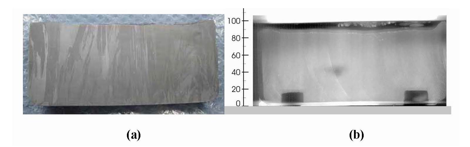
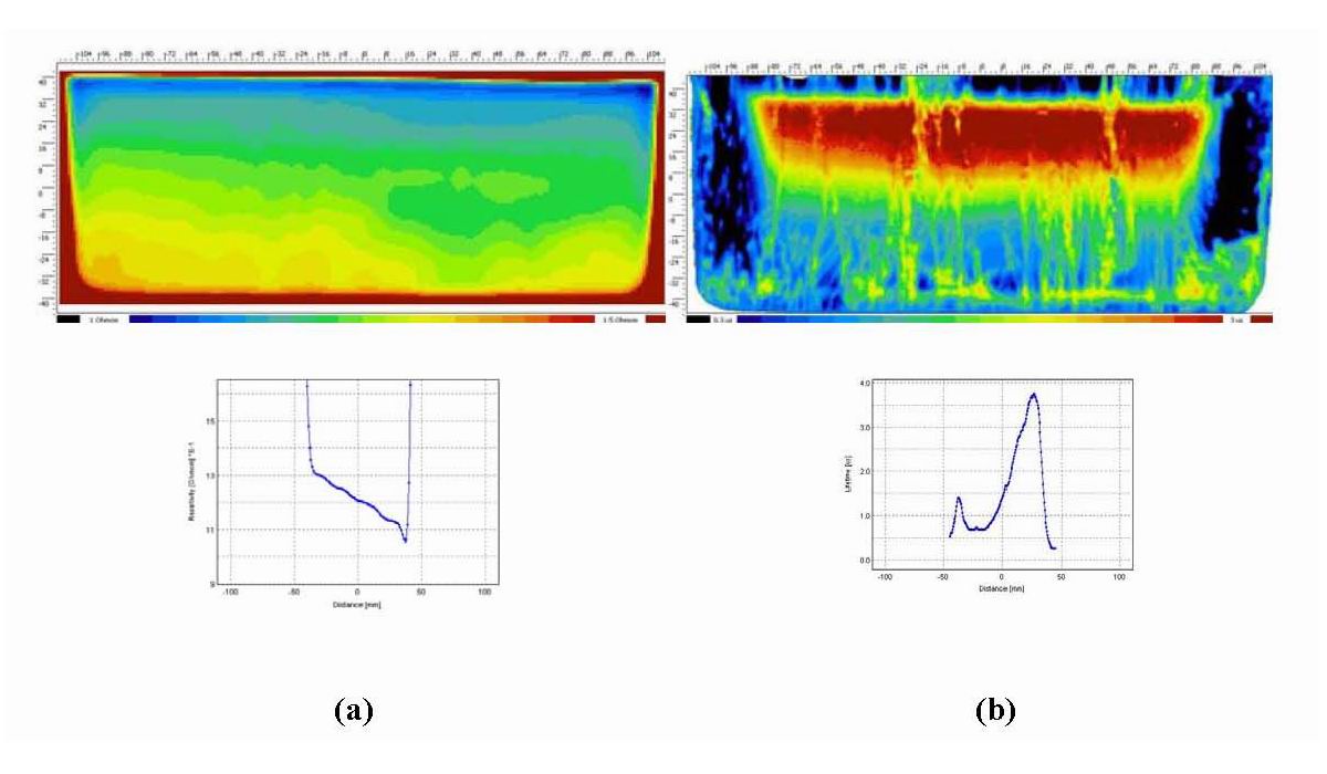
After solidification, the top part of the silicon block with the grown in graphite plate was removed by sawing for further investigation. Crystal structure visible at side cut of the solidified G1 block (see Fig. 1a) shows columnar growth with a sufficient grain size. Infrared transmission of Si below the graphite plate is presented in Fig. 1b. Only minor inclusions (probably SiC) at 40 mm height in the middle of the silicon block are observed. The two dark objects visible at the bottom of the material are the silicon nitride spacers. The desired range of resistivity between 1.3 and 1.0 Ωcm was achieved (see Fig. 2a), as well as acceptable μPCD-lifetime of the minority carriers (see Fig. 2b) being half as less again as the characteristics for standard blocks with high quality material. Besides probable introduction of impurities originated from the AHP model, the process was not adapted to using a floating plate.
FTIR and ICP-MS/NAA are correspondently applied to measure carbon and oxygen, as well as to analyze impurities in Si. Computer modeling has been applied for description of the thermal, convective and chemical transport processes during the growth run. The use of silica free crucibles is under discussion. The Si growth under these conditions may drastically change physical-chemical phenomena resulting in essential reduction of oxygen in silicon. 1. M.A. Gonik, A.I. Nepomnyaschih, V.V. Kalaev, A.D. Smirnov. Application of the Submerged AHP Heater for the Growing of the Multi-crystalline Silicon. Abstracts of the ACCGE-17 Conference, Lake Jeneva, Wisconsin, 2009. |
| Legal notice |
|
| Related papers |
Presentation: Poster at 17th International Conference on Crystal Growth and Epitaxy - ICCGE-17, Topical Session 5, by Michael A. GonikSee On-line Journal of 17th International Conference on Crystal Growth and Epitaxy - ICCGE-17 Submitted: 2013-03-28 17:15 Revised: 2013-07-18 13:01 |