| Search for content and authors |
Crystal growth of RbTiOPO4 epitaxial layers and optical waveguide applications |
| Ali Butt , Jaume Cugat , Rosa Solé , Maria Cinta Pujol , Joan J. Carvajal , Xavier Mateos , Jaume Massons , Francesc Díaz , Magdalena Aguiló |
|
FiCMA-FiCNA, Universitat Rovira i Virgili (URV), Marceli Domingo s/n, Tarragona 43007, Spain |
| Abstract |
| RbTiOPO4 (RTP) is an orthorhombic material, isostructural to KTiOPO4 (KTP), which crystallizes in the Pna21 space group [1]. It has high nonlinear optical and electrooptical coefficients, high damage threshold and chemical stability, which make it very interesting for optical and photonic applications [2]. RTP is a positive biaxial crystal with nx<ny<nz. It is known that the substitution of Rb by K in the RTP structure produces a decreasing of the refractive indices [2], which is interesting in order to obtain epitaxial layers of RbTiOPO4 on Rb1-xKxTiOPO4 useful for making waveguides (refractive indices of the epilayer higher that those of the substrate). On the other hand, the RTP doping with Yb and Nb produces an increasing of the refractive indices with respect to those of RTP, which makes possible to guide the light through an epitaxial layer of (Yb,Nb):RTP grown on a RTP substrate. The presence of Yb, as an active ion, allows the possibility to obtain self-frequency doubling at the same crystal.
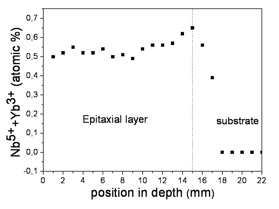
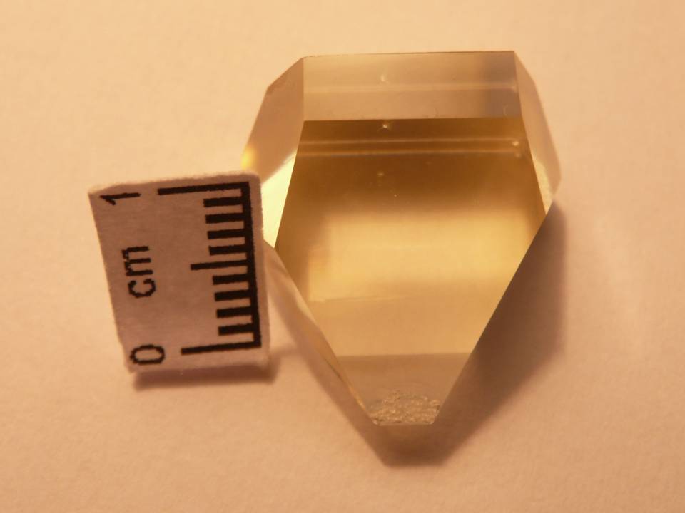
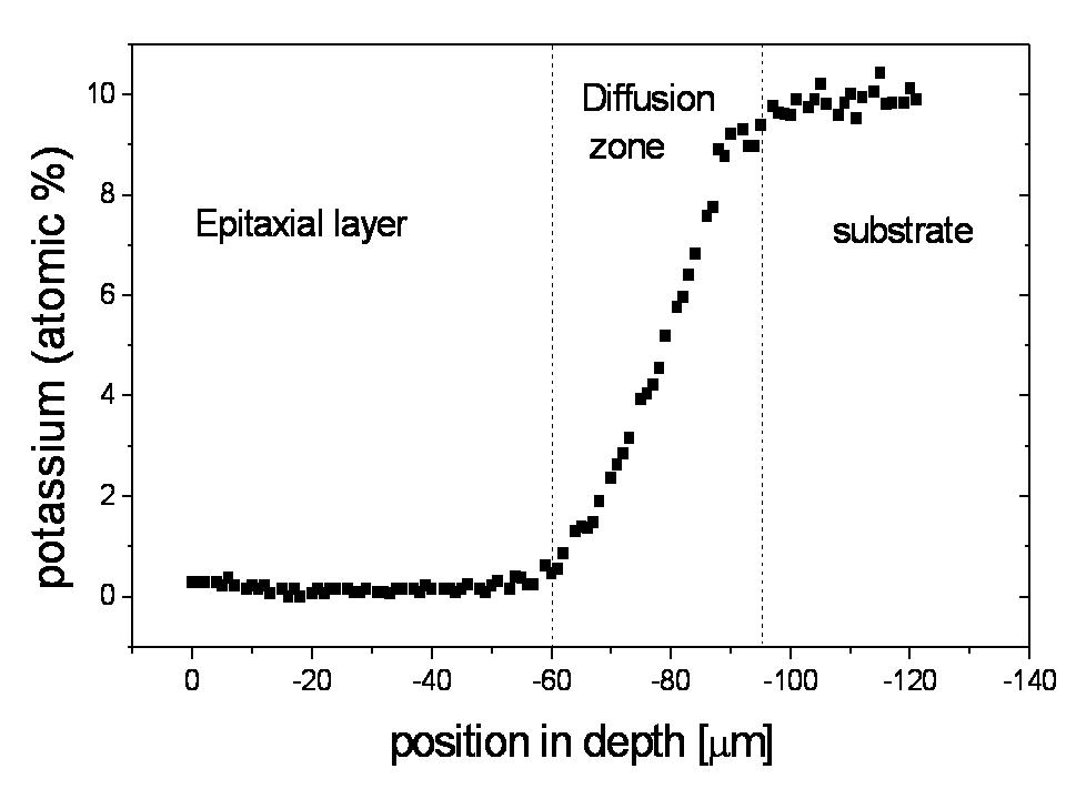
Thus, in this work, we have grown epitaxial layers of RTP on KRTP substrates and (Yb,Nb):RTP on RTP substrates in order to obtain planar waveguides. The crystals to be cut for substrates were grown from high temperature solutions using the top seeded solution growth technique. These crystals were cut in (001) oriented plates, which will be used as substrates. Figure 1 shows a RTP single crystal grown for substrates. The epitaxial layers were obtained by the liquid phase epitaxy technique. The first step was to determine accurately the saturation temperature of the solution for growing the epitaxial layers. After that, the substrates, previously cleaned, were slowly introduced into the furnace to avoid thermal shocks and maintained for about 30 min slightly above the surface of the solution. After that, the substrate was dipped in the solution at 1K above the saturation temperature for 5 minutes, followed by decreasing the solution temperature to 2 K down the saturation temperature, in order to grow the epitaxial layer for about 2 hours. During all the growth process, the crystal rotated at 65 rpm. After that, the crystal was removed from the solution, maintained at a few mm above the solution surface and the furnace was cooled slowly to room temperature. The doping concentration in the KRTP substrates and in the (Yb,Nb):RTP epitaxial layers and the concentration change through the substrate/epitaxial layer interface was measured by electron probe microanalysis. The unit cell parameters of the substrates and epitaxial layers were obtained from X-ray measurements. The refractive indices at room temperature and a wavelength of 632 nm were measured using the dark modes technique. In the RbTiOPO4/Rb1-xKxTiOPO4 (001) epitaxial layers, the lattice mismatch f(001) calculated using the formula f(hkl) = 100 x (S(hkl)(layer) – S(hkl)(substrate)) / S(hkl)(substrate) [3], was 0.303, while the nz refractive index contrast measured was 0.0047. The surface of the epitaxial layer showed in some parts, a capping effect due to the fast growth in the non natural face. The chemical composition of these single crystals grown for substrates was Rb0.9K0.1TiOPO4. EPMA analysis also showed K+ diffusion from the substrate into the epilayer with a non-sharp interface (Figure 2). This diffusion implies that these epitaxial layers can’t work as step-index waveguide, but graded index waveguide. In the RbTi1-x-yYbxNbyOPO4/ RbTiOPO4 (001) epitaxial layers, the lattice mismatch f(001) was 0.473 and the nz refractive index contrast was 0.0077. The chemical composition of the epitaxial layer measured by EPMA was RbTi0.958Yb0.016Nb0.026OPO4, with a distribution coefficient of Yb and Nb of KYb=0.14 and KNb=0.66, respectively. Figure 3 shows the composition change at the interface of a (Yb,Nb):RTP/RTP epitaxial layer. As can be seen in the figure, the Yb and Nb diffusion from the epitaxial layer to the substrate is only around 3 mm. This means that this kind of epitaxial layers can be used for fabricating step-index waveguides. Figure 4 shows the TM0 mode obtained by guiding the light through a (Yb,Nb):RTP/RTP planar waveguide.
Acknowledgements This work was supported by the Spanish Government under Projects MAT2011-29255-C02-02, TEC2010-21574-C02-02, by the Catalan Authority under Project 2009SGR235 and by the European Union under Project No. FP7-SPA-2010-263044. M. Ali Butt and J. Cugat thanks the Catalan Government and the Spanish Government for the funds provided through the FI-DGR fellowships.
References [1] P.A. Thomas, S.C. Mayo and B.E. Watts, Acta Crystallogr. B 48, 401 (1992). [2] M. N. Satyanarayan, A. Deeptly, H.L. Bhat, Critical Reviews in Solid State and Materials Sciences, 24, 103 (1999). [3] J. Cugat, R. Solé, J.J. Carvajal, M.C. Pujol, X. Mateos, F. Díaz and M. Aguiló, CrystEngComm, 13, 2015 (2011). Figure captions
Figure 1.- As-grown RTP single crystal
Figure 2.- K+ atomic concentration through the interface in a RTP/KRTP epitaxial layer
Figure 3.- [Nb5+,Yb5+] atomic concentration through the interface in a (Yb,Nb):RTP/RTP epitaxial layer 
Figure 4.- TM0 mode in (Yb,Nb):RTP/RTP planar waveguide |
| Legal notice |
|
| Related papers |
Presentation: Oral at 17th International Conference on Crystal Growth and Epitaxy - ICCGE-17, General Session 10, by Joan J. CarvajalSee On-line Journal of 17th International Conference on Crystal Growth and Epitaxy - ICCGE-17 Submitted: 2013-03-27 11:17 Revised: 2013-08-08 20:04 |
 .
.