| Search for content and authors |
Nanoporous GaN epitaxial layers grown by Chemical Vapor Deposition |
| Oleksandr V. Bilousov , Joan J. Carvajal , Xavier Mateos , Rosa Solé , Jaume Massons , Francesc Díaz , Magdalena Aguiló |
|
FiCMA-FiCNA, Universitat Rovira i Virgili (URV), Marceli Domingo s/n, Tarragona 43007, Spain |
| Abstract |
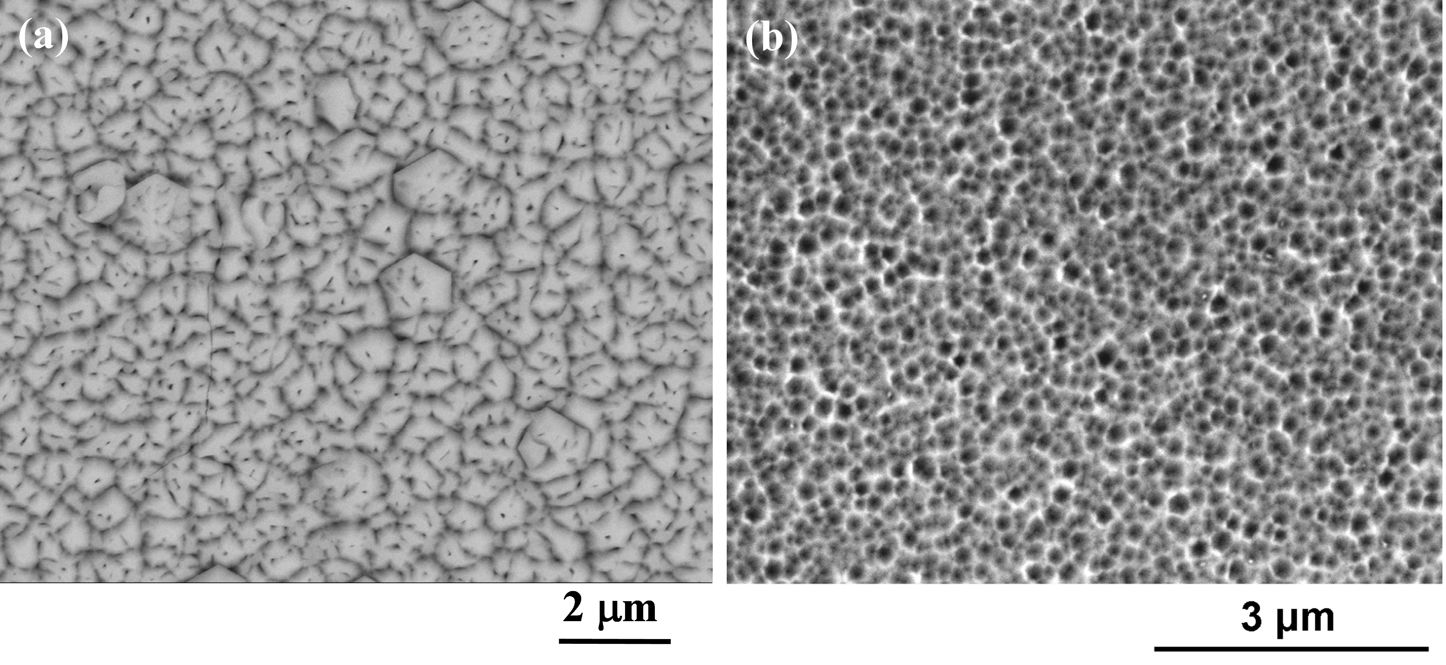
Hexagonal gallium nitride (GaN) is considered one of the most important wide band-gap semiconductors for a number of applications in electronics and optoelectronics. Porous GaN, due to its optical and electronic properties, is particularly interesting for developing optoelectronic devices with improved efficiency, such as LEDs with enhanced efficiency and sensors with enhanced sensitivity. Porous GaN has been typically fabricated by (photo)electrochemical and chemical etching methods. These methods generally suffer from a lack of control on the size, morphology and distribution of the generated pores. Thus, the poor reliability and reproducibility of these methods in the production of porous GaN had difficulted up to now the fabrication optoelectronic devices based on porous GaN. In 2009 we have shown that it was possible to produce nanoporous GaN microparticles in a simple chemical vapor deposition (CVD) system [1] without any secondary etching or chemical treatment after growth in order to generate the porosity. The porosity in these particles is only present on the (0001) face. Recently, we demonstrated that these nanoporous GaN particles can be deposited also on silicon substrates using a metallic catalyst, obtaining porous particles with a low density of defects, as revealed by the emission arising only from the band-edge of the particles obtained in the cathodoluminescence studies [2]. Also, by using this methodology of growth, we demonstrated the formation of low resistivity near ohmic Pt and Au metallic contacts on porous n-type GaN by the formation of intermetallic seed layers through the vapour-solid-solid (VSS) mechanism [3]. Using our method we started studying possibilities of orientation of nanoporous GaN along [0001] crystallographic direction, since it has potential interest for fabrication of LED with higher efficiency. As substrates for oriented growth of nanoporous GaN can be used hexagonal SiC and sapphire, since they crystallize in the same crystallographic systems with relatively small lattice mismatches, and also epitaxial GaN (0001). Here, we present an important step further in the crystal growth of nanoporous GaN, such it is the epitaxial growth of nanoporous GaN layers oriented along the [0001] crystallographic direction on epitaxial GaN (0001) substrates grown on sapphire substrates. In this way, all the pores of GaN are oriented along the same direction. We found that the lattice mismatch between the substrate and the porous GaN layer, plays an important role in order to obtain a continuous layer or a layer formed by discrete porous microparticles, as can be seen in Figure 1. The obtained porous GaN layers can be doped with magnesium (Mg) to get p-type conductivity, that combined with the inherent n-type of undoped porous GaN allows the fabrication of totally porous p-n junctions, with potential application in high brightness unencapsulated GaN-based light emitting diodes and sensors with high sensitivity.
Figure 1. SEM images of epitaxial porous GaN grown on (a) SiC and (b) GaN on sapphire substrates.
Acknowledgements This work was supported by the Spanish Government under Projects MAT2011-29255-C02-02, TEC2010-21574-C02-02, by the Catalan Authority under Project 2009SGR235 and by the European Union under Project No. FP7-SPA-2010-263044. O.V. Bilousov thanks the Catalan Authority for the funds provided through the FI 2011FI-B-00975 fellowship.
[1] J.J. Carvajal and J.C. Rojo, Crystal Growth Des., 9 (2009) 320. [2] J.J. Carvajal, O.V. Bilousov, D. Drouin, M. Aguiló, F. Díaz and J.C. Rojo, Microsc. Miocroanal., 18 (2012) 1. [3] O.V. Bilousov, J. J. Carvajal, D Drouin, X. Mateos, F. Díaz, M. Aguiló and C. O’Dwyer, ACS Appl. Mater. Interfaces 4 (2012) 6927. |
| Legal notice |
|
| Related papers |
Presentation: Oral at 17th International Conference on Crystal Growth and Epitaxy - ICCGE-17, Topical Session 3, by Joan J. CarvajalSee On-line Journal of 17th International Conference on Crystal Growth and Epitaxy - ICCGE-17 Submitted: 2013-03-27 09:51 Revised: 2013-07-23 17:26 |