| Search for content and authors |
Supphire Substrates With The Regular Relief Surface |
| Arsen Muslimov 1, Vladimir M. Kanevsky , Andrey Butashin , Alex Deryabin , Elena Rakova |
|
1. A.V.Shubnikov Institute of Crystallography The Russian Academy of Sciences, Moscow, Russian Federation |
| Abstract |
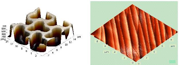
Application of the crystal substrates with the regular microrelief surface results in considerable reduction of the dislocation density in heteroepitaxial films like GaN on sapphire for example [1]. Such microrelief is usually created by the photolithography method and consequent etching of the substrate surface. Regular relief in a form of parallel steps and terraces of nanometer sizes can be created on the vicinal surface of sapphire substrates by their annealing in air at temperatures ≥1000ºC (Fig. 1.b). Application of such sapphire substrates with the regular nanorelief surface results in improvement of the crystal quality of the heteroepitaxial AIIBVI semiconductor films [2], and permits to form ordered ensembles of nanoparticles, like Au particles for example [3] on such surface. In present work regular microrelief on the sapphire substrate surface was created by following: - standard vacuum evaporation method to deposit the metal mask layer of about 0,35 µm in thickness; - standard photolithography method to obtained the windows of desired forms and sizes in the layer; - the Cl-ion reactive plasma etching of the surface in opened windows to the depth of about 1,5 µm. Obtained microrelief was formed by the circular or pseudo-triangle pits (Fig. 1.a) with the typical cut sizes 1÷7 µm and depths 1÷2 µm.
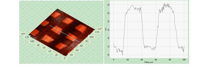
a b Fig. 1. AFM image of sapphire substrate surface with regular relief, created by the lithography and etching methods (a), and by annealing the vicinal (0001) sapphire substrate in air at 1400°С In addition experimental processes including vacuum deposition of Al metal on sapphire substrate surface through the regular pattern with the holes sizes 0.2÷40 µm and consequent oxidization and annealing were carried out to form regular microrelief on the surface (Fig. 2). Preliminary RHEED data, obtained from continuous film created by this method, indicate the film to be the sapphire single crystal. The jut lateral sizes are only defined by the pattern holes sizes, but the jut height does not exceed 20 nm for the moment, since it strongly depends upon the oxygen atoms diffusion length through the alumina layer from atmosphere to Al metal at its oxidization and the sapphire single crystal growth speed in the solid state as well.
a b Fig. 2. AFM image (a) and cross-section (b) of microrelief on the sapphire substrate surface, which is created by the vacuum deposition of Al metal through the regular pattern and consequent annealing at 1400°С in air This study was performed using the equipment of the Mixed-Use Center of the Institute of Crystallography, Russian Academy of Sciences (RAS), and supported by the Ministry of Education and Science of the Russian Federation and the RAS Presidium (Basic Research Program no. 24, “Fundamentals of the Technology of Nanostructures and Nanomaterials”). REFERENCES 1. Y. H. Kim, H. Ruh, Y. K. Noh, et. al. // J. Appl. Phys. 2010, V. 107, 063501. 2. V. I. Mikhailov, A. V. Butashin, V. M. Kanevsky, et.al. // J. Surf. Invest. 2011, Vol. 5, p. 595. 3. A. E. Muslimov, A. V. Butashin, A. A. Konovko, et. al. // Cryst Reports, 2012, Vol. 57, p. 415. |
| Legal notice |
|
| Related papers |
Presentation: Poster at 17th International Conference on Crystal Growth and Epitaxy - ICCGE-17, General Session 10, by Arsen MuslimovSee On-line Journal of 17th International Conference on Crystal Growth and Epitaxy - ICCGE-17 Submitted: 2013-03-26 10:54 Revised: 2013-07-17 22:28 |