| Search for content and authors |
Selective epitaxial growth of compressively strained Ge layers on Si in 40-nm trench arrays |
| Byongju Kim , Sun-Wook Kim , Hyunchul Jang , Jeong-Hoon Kim , Sangmo Koo , Dae-Hong Ko |
|
Yonsei University, School of Advanced Materials Science and Engineering, Seoul 120-749, Korea, South |
| Abstract |
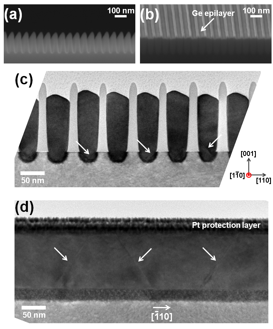
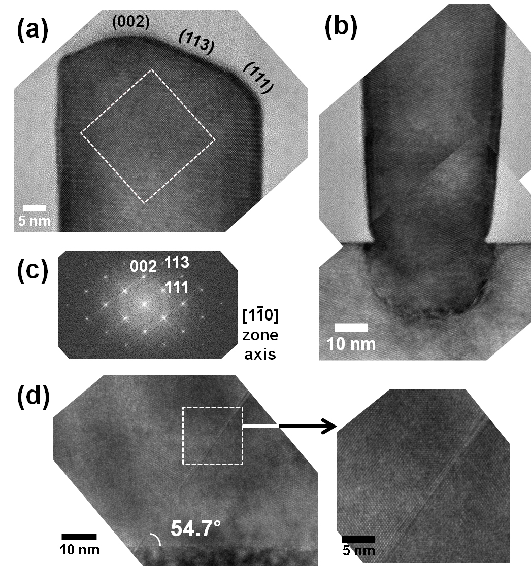
Because of the technical difficulties in manufacturing nano-scaled semiconductor devices and also the inherent property of a low mobility, Si is not adequate for next generation high speed complementary metal oxide semiconductor (CMOS) logic devices beyond 10 nm nodes. In order to overcome these limitations, many researchers have explored Ge in order to replace Si for p-channel materials owing to its high hole mobility of 4 times higher than that of Si [1-4]. Despite such a merit of achieving high speed, the issues of a high cost of Ge wafers and the compatibilities with conventional Si CMOS processes have limited Ge’s applications for replacing conventional Si channels. Although the epitaxial growth of the strain-relaxed Ge layers on Si wafers somewhat provides resolution from an economic perspective, high defect density in the Ge layers as well as their rough surfaces due to its large lattice mismatch of 4.2% with Si do not allow the integration of the Ge channel on Si substrates. The aspect ratio trapping (ART) process, which involves selective growth of Ge on the Si regions between SiO2 trench walls, has recently been reported to significantly reduce the magnitude of the defect density in the epitaxial Ge layers [5-11]. Despite the successful demonstration of the epitaxial Ge layers by ART process in the wide trenches and discrete holes, the fundamental understanding of the defect generations in the Ge layers in the narrow trenches have not been investigated, yet [6-11]. Indeed for the application to the nano scale Si devices, this issue of the buildup of the residual strain and consequent defect formations should be resolved. Therefore an in-depth research on the Ge growth in narrow (< 50 nm) trench arrays is needed. In this paper we report the fabrication of high quality and compressively strained Ge epilayers on Si substrate using ART technology with a template of 40 nm SiO2 trench array patterns. The cross-sectional shape of Ge layers was monitored by scanning electron microscopy (SEM) (JEOL, JSM-7001F). High resolution transmission electron microscopy (HR-TEM) measurements were carried out using a JEOL JEM-2100F. In order to analyze the strain in the Ge layers nanobeam electron diffraction (NBD) measurement was performed using TEM with a 2.5 nm diameter probe size. Figures 1(a) and 1(b) depict the SEM images of the 40-nm-width trench arrays before and after the deposition, respectively. As can be seen in Fig. 1(b), Ge layers in each trench were deposited on a Si substrate with a uniform surface. Figures 1(c) and 1(d) show the cross-sectional TEM images of Ge epilayers. In Figure 1(c) the cutting direction of the sample was [110], which is perpendicular to the direction of trenches and the Ge sample was prepared by the conventional ion milling method. Figure 1(d) shows the TEM image of the Ge specimen prepared by focused ion beam method along the trenches to reveal a single Ge epilayer. Despite a large lattice mismatch Ge was grown epitaxially with a low defect density. In a Ge/Si system, the critical thickness to nucleate a dislocation at the interface is estimated to be ~ 10 Å [11]. Therefore there are misfit dislocations at the Ge/Si interfaces that propagate to Ge epilayers forming threading dislocations. Since Ge has a diamond cubic crystal structure, its Burgers vector is b = a/2<110> and dislocations formed glide on (111) planes [12]. In addition, stacking faults are observed on the (111) planes with an angle of 54.7° to Si surface indicated by arrows as shown in Figs. 1(c) and 1(d). Nevertheless an upper region of Ge layers, of which heights are larger than critical thickness, reveals defect-free regions and top surface is formed with side facets. In order to investigate the crystal quality, HR-TEM analyses were performed. Figures 2(a) and 2(b) show the HR-TEM images of the Ge epilayer inside the SiO2 walls at upper region and in the vicinity of the Ge/Si interface, respectively. It is noted that the Ge layer was epitaxially grown with bottom Si substrate. Based on the diffraction pattern obtained from the dashed rectangular area in Fig. 2(a), we conclude that the Ge epilayer is surrounded by simultaneously flattened (001), (113), and (111) facets, as shown in Fig. 2(c). The epitaxial growth is also confirmed in the direction parallel to the trench [-110] (See Fig. 2(d)). In this case, as mentioned before, there are the stacking faults propagating from the Ge/Si interface to Ge top surface while maintaining a regular interval. Figure 2(d) displays clearly that the stacking fault is on the (111) plane making an angle of 54.7°. Despite the large lattice mismatch and the condition where the height of Ge films is well above the critical thickness, a defect density is lower than expected and no surface roughening is observed as compared to the growth of Ge on bare Si wafers. It is likely that in the case of growing Ge layer in a narrow trench, SiO2 mask prevents misfit dislocations from gliding to the side due to the constraint of lateral space along [110]. We attribute the low defect density of Ge to the growth of compressively strained layer. In order to measure the residual strain we performed the NBD analyses and these results will be presented in the conference. Due to an increasing demand on high mobility devices and a low cost strategy, Ge has been grown on Si substrates in SiO2 trenches using ART technology. Starting with a SiO2 trench array pattern with a width of ~ 40 nm, we obtained high quality Ge epilayers with a low defect density despite the lattice mismatch of 4.2% between Ge and Si. HR-TEM analyses demonstrate that threading dislocations are located in a lower region of Ge epilayers and at regions above that the defect-free Ge layers are achieved.
Figure 1. SEM images of the Ge trench patterns (a) before the deposition and (b) after the deposition, TEM images of Ge epilayers along two mutually perpendicular directions (c) [110] and (d) [-110], showing the defects indicated by the arrows
Figure 2. HR-TEM images of the Ge epilayer (a) at top region, (b) in the vicinity of the Ge/Si interface, (c) diffraction pattern for the selected area indicated by the dashed rectangle in (a), and (d) HR-TEM image of the Ge epilayer along the direction of the trench, showing the stacking fault and an enlarged atomic-scale view References [1] Minjoo L. Lee et al., Appl. Phys. Lett. 79, 3344 (2001). [2] C. O. Chui et al., Tech. Dig. - Int. Electron Devices Meet. 2001, 437. [3] Donald A. Neamen, Semiconductor Physics and Devices: Basic Principles 4th ed., (McGraw-Hill, New York, 2012). [4] Darin Leonhardt et al., J. Appl. Phys. 110, 073516 (2011). [5] E. A. Fitzgerald et al., J. Electron. Mater. 20, 839 (1991). [6] T. A. Langdo et al., Appl. Phys. Lett. 76, 3700 (2000). [7] J.-S. Park et al., Appl. Phys. Lett. 90, 052113 (2007). [8] J. Bai et al., Appl. Phys. Lett. 90, 101902 (2007). [9] D. Pawlik et al., Electron. Lett. 44, 930 (2008). [10] G. Wang et al., J. Appl. Phys. 108, 123517 (2010). [11] J. W. Matthews et al., Thin Solid Film 33, 253 (1976). [12] D. Hull et al., Introduction to Dislocations 5th ed., (Elsevier, New York, 2011). |
| Legal notice |
|
| Related papers |
Presentation: Poster at 17th International Conference on Crystal Growth and Epitaxy - ICCGE-17, General Session 10, by Byongju KimSee On-line Journal of 17th International Conference on Crystal Growth and Epitaxy - ICCGE-17 Submitted: 2013-03-21 09:02 Revised: 2013-04-15 16:03 |