| Search for content and authors |
Fabrication of large-area Si-based photonic nanostructures coupled with Ge quantum dots and their application to solar cells |
| Noritaka Usami 1, Yusuke Hoshi 1, Takanori Kiguchi 2, Kazufumi Ooi 3, Takeshi Tayagaki 3 |
|
1. Graduate School of Engineering, Nagoya University, Furo-cho, Chikusa-ku, Nagoya 464-8603, Japan |
| Abstract |
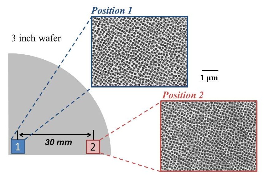
Photonic crystals or nanostructures are regarded as promising in the field of optoelectronics since they could control and manipulate photons. Management of photons is of great importance also in solar cells. However, application of photonic nanostructures to solar cells has been considered to be not feasible. This is due to the fact that fabrication of photonic nanostructures generally requires advanced lithography techniques and is limited to a small-area. It would be ideal if one could fabricate large-area photonic nanostructures without any lithography techniques so that one can implement photonic nanostructures to solar cells. We show that lateral modulation in strain in vertically aligned Ge quantum dots leads to modulation in the etching rate against a chemical solution. This could be utilized for fabrication of Si-based large-area photonic nanostructures coupled with Ge quantum dots without any lithography techniques.
The photonic nanostructures could change optical properties. In fact, we observed that photoluminescence intensity of Ge quantum dots is drastically increased by the presence of the photonic nanostructures. Furthermore, the conversion efficiency of the solar cell with photonic nanostructures was found to be slightly higher than that of the control Si solar cell with a flat surface. |
| Legal notice |
|
Presentation: Poster at 17th International Conference on Crystal Growth and Epitaxy - ICCGE-17, Topical Session 5, by Noritaka UsamiSee On-line Journal of 17th International Conference on Crystal Growth and Epitaxy - ICCGE-17 Submitted: 2013-03-20 09:34 Revised: 2013-04-14 12:12 |