| Search for content and authors |
Growth and multiple stacking of self-assembled InGaAsN/GaP quantum dot by molecular beam epitaxy |
| Noriyuki Urakami 1, Hironari Ito , Hiroto Sekiguchi , Hiroshi Okada , Akihiro Wakahara |
|
1. Toyohashi University of Technology, Toyohashi Hibarigaoka, Tempaku-cho, Toyohashi, Aichi 441-8580, Japan |
| Abstract |
|
Introduction:
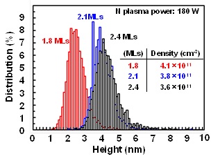
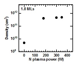
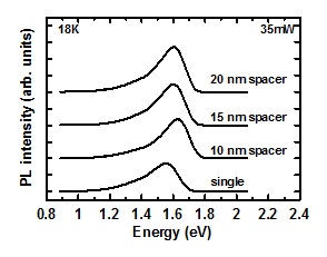
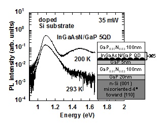
For the realization of future high integration optical interconnection devices such as optoelectronic integrated circuits, monolithic integration of III-V based optical devices to Si is key technology because Si has indirect band gap [1]. In particular, the conventional III-V based optical materials like GaAs or InP with low densities of crystalline defects such as threading dislocations and misfit dislocations are necessary to achieve long device lifetime. The dilute nitride GaAsPN (As > ~ 80 %) alloys shows direct band gap and is promising for the pseudomorphic quantum well grown on Si substrate [2]. However, high N incorporation (~ 7.5 %) into the GaAsPN/GaP QW structure has been designed to obtain conduction band offset (ΔEc) and to close the lattice constant to that of Si, because conduction band energy and lattice constant of dilute nitride decrease with the increase of N composition. Point defects related N incorporation have increased with the increase of N composition in the dilute nitride [3]. Point defects generally act the nonradiative recombination centers. On the other hands, InGaAs/GaP quantum dot (QD) structure has been investigated for Si-based optical devices [4]. This structure has been expected higher carrier confinement and temperature stability compared to QW structure, because QD structure can been available to three-dimensional carrier confinement. However, low carrier confinement has been reported by band alignment calculation due to GaP barrier layer is indirect semiconductor and highly compressive strain applies to InGaAs [5]. Therefore, the increase of ΔEc is necessary in order to realize high performance optical devices. The N incorporation into InGaAs QD is one of candidates to achieve higher ΔEc. Here, it should be noted that N incorporation into QD structure may impact a growth behavior of three-dimensional islands such as size distribution reported InAsN/GaAs QD systems [6]. In this report, effects of N incorporation on form characterizations of self-assembled InGaAsN/GaP QD islands were investigated. The size fluctuation of islands height was optimized narrow by deposition thickness and N composition. Additionally, since critical thickness for GaP layer on Si substrate without misfit dislocation has been 50 – 70 nm [7], the GaP spacer layer in multiple stacked InGaAsN/GaP QD structure was studied as thin as possible by observation of luminescence spectra. Lastly, growth of the multiple stacking InGaAsN/GaP QD structure on Si substrate was demonstrated. Experimental produce: Self-assembled InGaAsN/GaP QDs were grown by a conventional solid-source molecular beam epitaxy apparatus equipped with an As2 valved cracker and radio frequency (rf)-plasma N cell. We used semi-insulating GaP (001) substrates. The growth temperature, growth rate and beam equivalent pressure (BEP) ratio of BEPAs2/BEP(In+Ga)were set to 460 ºC, 0.3 monolayers per second (ML/s) and 20, respectively. The In composition was fixed 40% which was estimated by InGaAsN/GaAs QW. In the first step, uncapped InGaAsN/GaP QDs were fabricated to investigate islands density and height distributions. Prior to the growth of InGaAsN islands, a 100-nm thick GaP buffer layer was grown at 600 ºC. Subsequently, we switched the group-V beam from P2to As2. Then the substrate temperature was reduced to 460 ºC, self-assembled InGaAsN islands were formed by Stranski-Krastanov growth mode. After the growth, the substrate was rapidly cooled under As2irradiation in fabrication of uncapped samples. After the self-assembled InGaAsN islands formed as mentioned above, islands were embedded with a 20-nm thick GaP at 460 ºC in fabrication of GaP-capped to observe luminescence spectra. Where, to suppress the reduction of the density on the embedded islands by As/P exchange reactions, Ga adatoms corresponding to approximately 1 ML was deposited on the islands before P2 beam supply [8]. The substrate temperature was then taken to 580 ºC and a 80-nm thick GaP layer was grown. The deposition thickness was 1.8 ~ 2.4 MLs. The N plasma power of N cell was 180 ~ 350W and N2 flow rate was fixed 0.1 sccm. In the next step, GaP spacer layers thickness in the multiple staked InGaAsN/GaP QD structure were investigated. The GaP spacer layers thickness were investigated from 10 to 20 nm by the double stacked QD structure. Then, deposition thickness and N plasma power were 1.8 MLs and 180 W in a QD layer, respectively. Lastly, the five stacked InGaAsN/GaP QD structure on the dislocation free GaP/Si template was fabricated. The GaP/Si template was developed by migration enhanced epitaxy with optimized conditions with growth sequence and annealing [7]. Then, the GaP spacer layers thickness in the QDs structure were 10nm. The surface images of InGaAsN/GaP QD islands were characterized by atomic force microscopy. Photoluminescence (PL) spectra were measured by pumping with a 532-nm Nd: YVO4 laser. Results and discussion: Figure 1 shows amount of deposition dependence of height distribution on uncapped InGaAsN/GaP QD islands. The islands density was realized 1011 cm-2 in all samples as shown in the inset. Especially, high islands density of 4.1×1011cm-2 was available with 1.8 MLs deposition. This density is approximately 3 ~ 4 times higher than that of conventional self-assembled QD systems such as In(Ga)As on GaAs (001) substrates. Since the height fluctuation generally affects line width of luminescence spectrum, narrow height fluctuation is desired. The height fluctuation for 1.8 MLs deposition was the narrowest in this study and, then the average height was 2.6 nm. Figure 2 shows dependence of N plasma power on islands density of uncapped InGaAsN/GaP QD islands. The inset table shows islands density. In the GaAsN/GaP quantum well systems, the N composition of each samples were estimated to be 1.2, 2.5 and 3.0 % with N plasma power of 180, 300 and 350 W, respectively. The islands density grown with supplying N radicals was two orders higher than that without supplying N radicals. Migration length of In and Ga adatoms were decreased with supplying N radicals due to bonding energy of III-N are higher than that of III-As. Additionally, islands density and height distribution seems to be not depend on N plasma power. Here, N incorporation efficiency with compressive strain material systems has been shown the increase compared to unstrained material systems in dilute nitride. For GaPN alloys, the N composition grown on Si substrate has been increased 1.6 times more efficient compared to GaP substrate [9]. Therefore, plasma power of 180 W is sufficient. Figure 3 shows dependence of GaP spacer layer thickness on PL spectra from InGaAsN/GaP double stacked QD and single QD. The PL peak energy blueshifted with thinning the GaP spacer layer reducing from 20 nm to 10 nm. The mini-band formation caused by electron coupling in vertical direction was not dominantly indicated. If the mini-band formation occurred, the red-shift should be observed [10]. This finding was attributed to the increase of lateral compressive strain with thinning the GaP spacer layer [11]. On the other hand, PL intensity from double staked QD samples for any spacer thickness was monotonically increased approximately 1.5 times compared to single QD. Thus, the spacer layer thickness could be thinned to 10 nm without the degradation of PL intensity. From the above results, the deposition thickness, N plasma power and spacer thickness in the multiple stacked InGaAsN/GaP QD structure on GaP substrate were optimized to 1.8 ML, 180 W and 10 nm, respectively. Figure 4 shows luminescence spectra of InGaAsN/GaP 5QD structure on GaP/Si template and sample structure, respectively. This structure was consisted In0.4Ga0.6AsN/GaP 5QD active layer and GaP0.97N0.03 barrier layer. In order to improve luminescence intensity, the sample was performed thermal annealing in N2 ambient for 1 minute at 700 ºC. Two different luminescence peaks from doped-Si substrate and InGaAsN/GaP 5QD were observed at 200 K. However, luminescence from InGaAsN/GaP 5QD was not observed at 293 K. The increase of active non-radiative recombination centers in the layer structure with rising measurement temperature was one of the reasons. In particular, many deep traps which are like isoelectronic traps existed in InGaAsN QD layers and the crystalline was not completely improved by annealing above. Additionally, InGaAsN QDs were selectively excited in active layer of InGaAsN/GaP 5QD structure because the absorption coefficient of GaP crystal is 1.25 ×10⁻² cm-1 at 532-nm (2.33 eV) and absorption of GaP at the energy region is weak [12]. References [1] H. Yonezu, Semicond. Sci. Technol. 17 (2002) 762. [2] B. Kunert, et al., Appl. Phys. Lett. 88 (2006) 182108. [3] I. A. Buyanova, et al., Solid-State Electron. 47 (2003) 467. [4] T. N. Thanh, et al., Appl. Phys. Lett. 99 (2011) 143123. [5] F. Fukami, et al., Phys. Stat. sol. C 8 (2011) 322. [6] J. F. Fälth, et al., Nanotechnology 19 (2008) 045608. [7] K. Yamane et al., J. Cryst. Growth 312 (2010) 2179. [8] K. Umeno et al., Physica E 42 (2010) 2772. [9] A. Utsumi et al., J. Cryst. Growth 295 (2006) 12. [10] G. S. Solomon et al., Phys.Rev.Lett.76 (1996) 952. [11] Q. Xie, et al., Phys.Rev.Lett.75 (1995) 2542. [12] S. Adachi, Optical Constants of Crystalline and Amorphous Semiconductor, Kluwer Academic Publishers, United States of America, 1999.
Figure 1. Amount of deposition dependence of height distribution for uncapped samples. The inset table shows islands densities.
Figure 2. Dependence of N plasma power on islands density for uncapped samples.
Figure 3. PL spectra at 18 K as a function of spacer layer thickness.
Figure 4. PL spectra at 200 and 293 K from InGaAsN/GaP 5QD on GaP/Si template. Inset shows layer structure. |
| Legal notice |
|
Presentation: Oral at 17th International Conference on Crystal Growth and Epitaxy - ICCGE-17, General Session 8, by Noriyuki UrakamiSee On-line Journal of 17th International Conference on Crystal Growth and Epitaxy - ICCGE-17 Submitted: 2013-03-02 07:53 Revised: 2013-07-24 20:12 |