| Search for content and authors |
EUMINAfab: Micro and nano fabrication technologies for optical and sensor applications |
| Jorge Ramiro , Santos Merino , Sabino Azcárate |
|
Fundación TEKNIKER (TEKNIKER), Avda. Otaola, 20, Eibart 20600, Spain |
| Abstract |
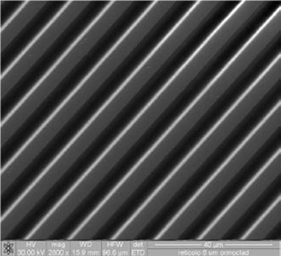
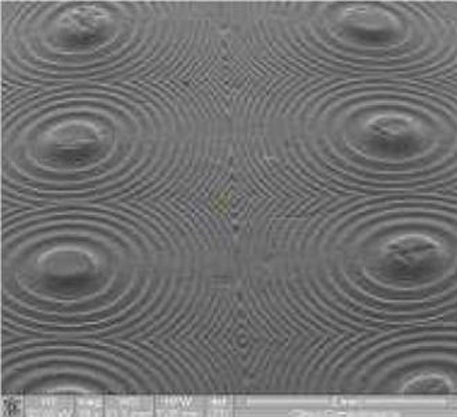
Technologies for optical and sensor fabrication are numerous and specific for each particular design. They comprise processing of silicon, compound semiconductors, glass, metals, ceramics and plastics. EUMINAfab (http://www.euminafab.eu) offers installations capable of processing all these materials, including amongst other equipment, micro and nanostructuration, deposition of thin and thick films and replication technologies. In addition, the quality of the fabricated devices can be assessed using the characterization equipment available in this platform. Technologies for optical applications Micro- and nanooptics are optics (lenses, prisms, mirrors,...) that have structures smaller than one millimetre or one micrometre in order to reflect, refract and diffract the light. Since the shapes and features of these optics must be controlled to very small scales in order to manipulate the light in the way we want, micro and nano fabrication technologies and processes that fit these high requirements must be used. Lithography is the most important technological approach for microoptics fabrication. It is composed of a sequence of processing steps to structure the surfaces of planar substrates. Two types of lithographic fabrication procedures can be distinguished, mask lithography and scanning lithography. In mask lithography, the pattern of the optical component is encoded as an amplitude distribution in a lithographic mask. Uniform illumination of the mask is used to expose a photosensitive coating on the substrate. In scanning lithography no masks are used. Local variation of the photoresist exposure is achieved using a direct writing process. After the exposure of the photoresist layer a development step converts the exposed photoresist into a surface profile. In a further processing step, the surface profile of the photoresist pattern can be transferred into the substrate. Regarding mask lithography, two partners (Tekniker and Centro Ricerche FIAT, CRF) offer their UV photolithography equipment. An example of a diffractive grating fabricated using this approach is shown in Figure 1.
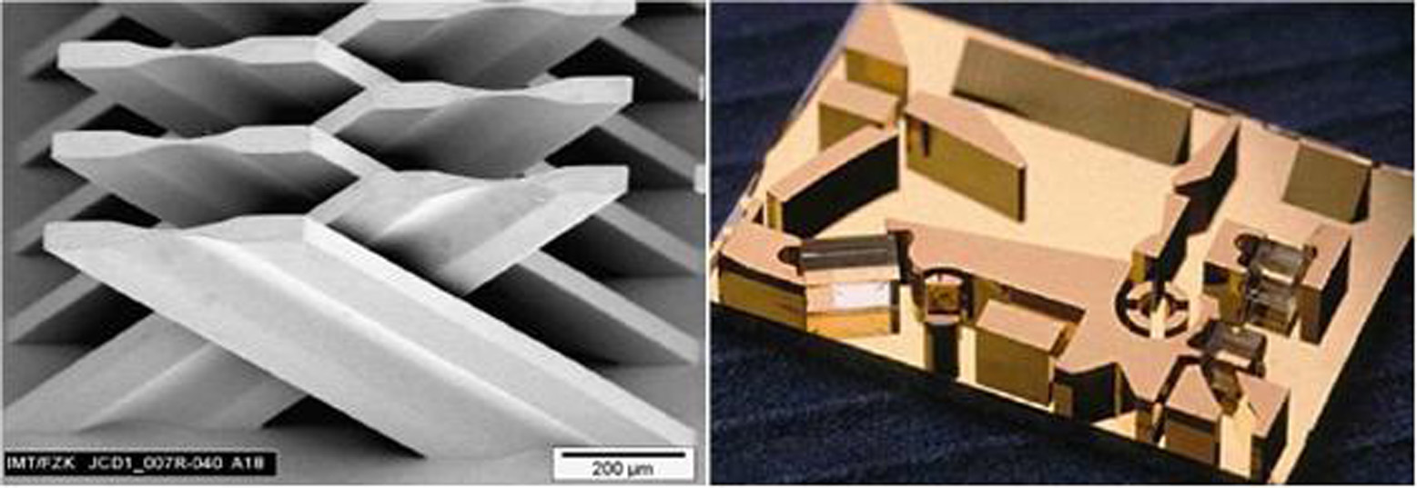
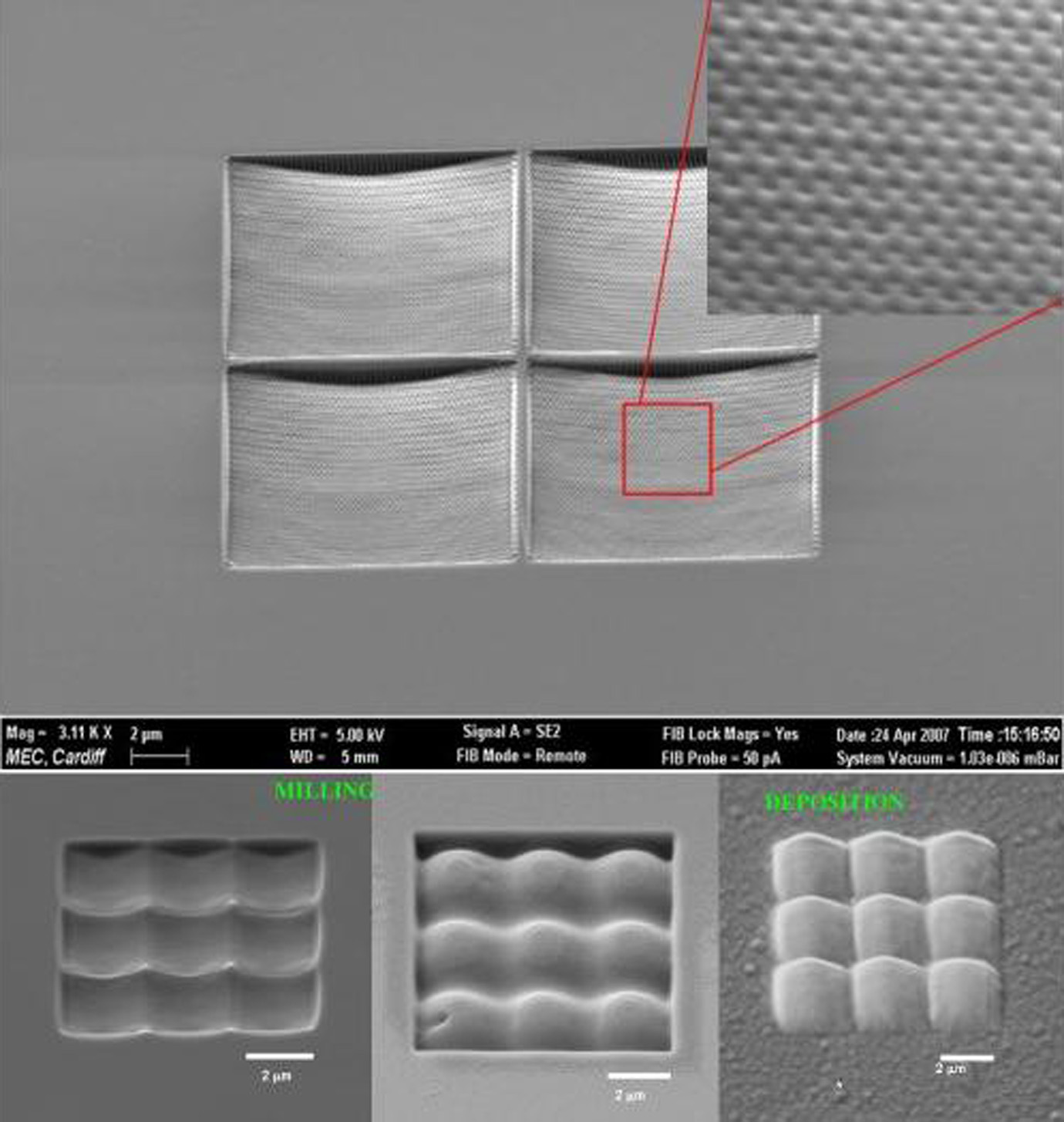
Figure 1. Diffractive grating with 6 µm pitch Instead of using optical light sources for exposing the substrate, it is possible to use other types of radiation, such as x-rays. Karlsruhe Institute of Technology (KIT) makes available its deep x-ray lithography facilities, which use synchrotron radiation to pattern thick PMMA layers (up to several millimetres). Due to the extremely short wavelengths, the diffraction effects are reduced and the resolution is enhanced. Due to the high penetration depths and small diffractive beam widening, this lithographic technique allows the fabrication of deep structures with high aspect ratios (up to 50). The structures are characterized by very steep sidewalls, with sidewall roughness in the range of 20-30 nm. This potential is very interesting for the fabrication of refractive microoptical components. Figure 2 shows some examples of optical devices fabricated using this equipment. Figure 2. (Left) Crossed X-ray lenses made in SU-8. (Right) Microoptical bench with cylindrical mirrors and fixing structures Regarding scanning lithography, two different kinds of direct writing processes are available in EUMINAfab, focused ion beam (FIB) and electron beam. Cardiff University offers its FIB/SEM CrossBeam, which consists of an emission gun electron column and a high performance Ga+ FIB column. The system allows machining of complex 3D structures, like those shown in Figure 3, through ion sputtering and/or gas assisted etching and deposition.
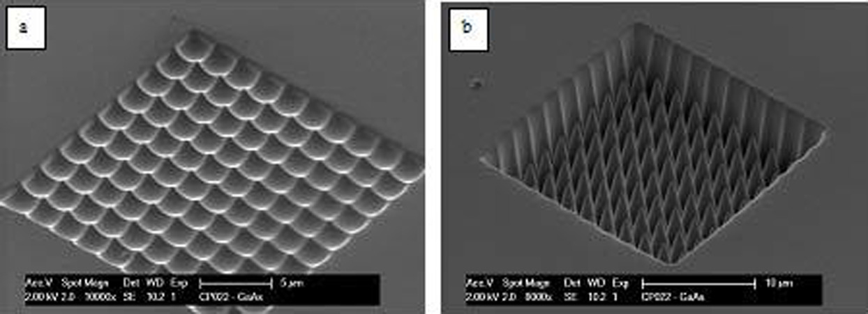
Figure 3. (Top) Micro lens array with nano surface structures in fused silica. Each lens is 12 x 12 microns and the nano lenses are 120 nm in diameter. (Bottom) SEM images of arrays of 2x2 µm micro lenses It is also available in EUMINAfab the CHARPAN equipment (Charged particle nanopatterning with massively parallel ion multibeams, located at IMS), which provides 43000 programmable beams with a size of 12.5 nm at the substrate, opening new ways for micro and nanooptics. Figure 4 shows examples of single-step fabrication of Si and GaAs microlenses using this equipment (borosilicate microlenses can also be fabricated).
Figure 4. 10 x 10 array of (left) convex microlenses on silicon and of (right) concave microlenses on GaAs Regarding electron beam, two installations can be used, one at MiPlaza and another at KIT. Electron beams have the advantage of consisting of charged particles which can be influenced by electric and magnetic fields, and the wavelength is even shorter than that for x-rays. The drawback is that it is a relatively time consuming and expensive technology for pattern generation. Therefore, it is mainly used in the fabrication of masks for lithography, or in the fabrication of masters for alternative methods, so that the most expensive process is only used once and the pattern can be copied many times onto the substrate. Anyway, in combination with replication techniques, electron beam can be an interesting approach to fabricate both refractive and diffractive optical elements. EUMINAfab also has other alternative lithographic approaches in order to structure substrates for optical applications, such as soft lithography or nanoimprint lithography present at the installations of CRF (Figure 5) and Tekniker. In these techniques a polymer is printed, and the printed polymer can be used as an etch mask or as the fabricated device. A high resolution is obtained (<10 nm lateral size [1]), and some commercial applications have been developed in the last years, such as near-IR polarizers for telecommunication, visible polarizers for projection displays, optical waveplates for optical pickup units, LEDs with enhanced light brightness, microlens arrays and diffractive optical elements, multilayer integrated optics and optical storage [2].
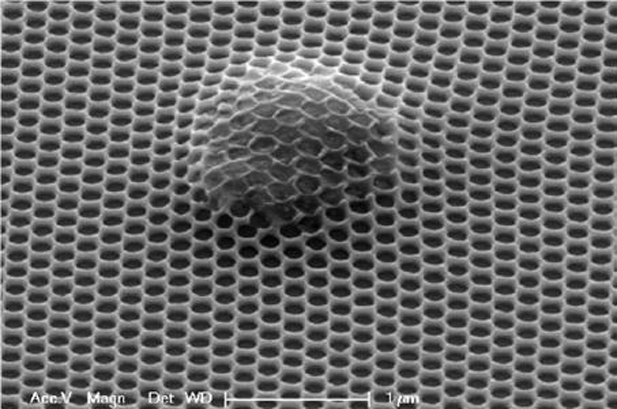
Figure 5. Array of Fresnel lenses with a relief height of 40 µm and a minimal depth of 10 µm These alternative approaches are not limited only to flat substrates. MiPlaza makes available its equipment for substrate conformal imprint lithography (SCIL), which offers the possibility to do large area printing, even on non-flat surfaces and over topography, as can be seen in Figure 6.
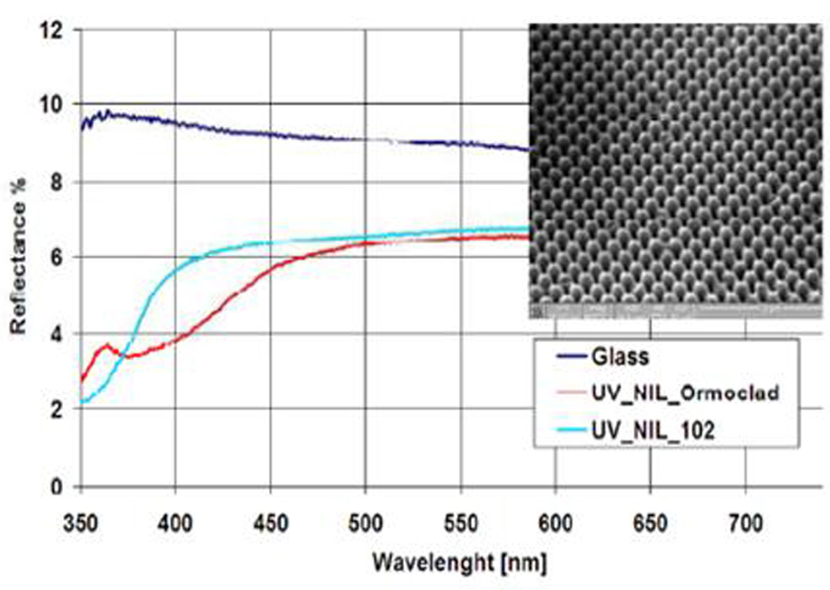
Figure 6. SCIL patterned honeycomb grid The transfer of the photoresist pattern to the substrate can be done by etching. This can be carried out using the DRIE and RIE equipment available in EUMINAfab. Besides lithographic fabrication processes, EUMINAfab offers laser (Cardiff University) and micromachining processes that could be useful for optical applications. There are examples in literature of the use of laser micromachining in the fabrication of diffractive optical elements and waveguides [3]. In addition, mechanical micromachining (present at KIT, Cardiff University, and Tekniker installations) such as diamond turning is an interesting alternative for the fabrication of microoptical elements when deep surface-relief are required or for blazed diffractive elements [3]. Replication techniques (like hot embossing or micro-injection moulding) of microoptical elements are important for mass production (e.g. reflective holograms on credit cards [3]) and are available in EUMINAfab. The moulds can be fabricated using the aforementioned techniques, or an additional step of electroforming (also available) can be added in order to obtain a tougher mould made in nickel. In addition to micro and nanostructuring, EUMINAfab offers a number of different techniques for deposition of thin films (PVD, different kinds of CVDs,...) which can be helpful for optical applications. One of the main applications of these techniques is for anti-reflective coatings which can be applied to the surface of lenses in order to reduce unwanted reflections. Finally, to characterize the quality of fabricated microoptical components, physical (lateral and depth dimensions, shape of the profile, surface roughness) and optical parameters can be assessed. A number of physical characterization techniques (mechanical perfilometry, AFM, electron microscopy, confocal imaging, interferometry, ellipsometry, ...) are available in EUMINAfab and one partner (CRF, Figure 7) has an installation dedicated to electro-optical characterization.
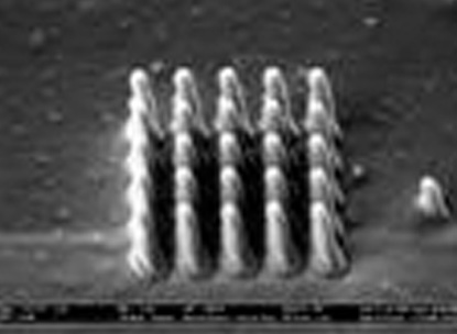
Figure 7. Reflectance measurements of antireflective nanostructures Technologies for sensor applications A sensor is a device that receives a stimulus (a physical quantity) and converts it into a signal (usually electrical). Sensors can be used to measure mechanical quantities (position, displacement, acceleration, force, flow rate,...), thermal quantities (temperature, flux, thermal heat,...), viscosity, radiation intensities, electrostatic and magnetic magnitudes (fields, charge, conductivity, permeability,...) and also chemical (component identities, concentrations,...) and biological (concentration of antigens, antibodies,..) quantities [4]. Different effects are used to convert the stimulus into a signal (pyroelectricity, piezoelectricity, Seebeck effect, Hall effect, …) and they depend on the properties of materials. The materials used to fabricate sensors could be semiconductors, glasses, metals, ceramics and polymers. Methods of sensor fabrication are numerous and depend on the material and on the particular design. Silicon possesses a large number of effects (Hall effect, piezoresistance, Seebeck effect,..) which are useful for sensor applications. In addition, it exhibits interesting mechanical properties which currently are widely used to fabricate devices such as pressure transducers, temperature sensors and force and tactile detectors, using processes like those shown in the previous section. Instead of single crystalline silicon, using polysilicon allows to develop sensors with unique characteristics. Polysilicon thin films on glass can be deposited thanks to the low temperature polysilicon line available in MiPlaza that employs a technology by which amorphous silicon is recrystallized. The use of this technology can be useful for the fabrication of temperature and fingerprint sensors. Regarding polymers, poly(vinyl fluoride) (PVDF) and related copolymers, are semicrystalline materials with strong piezoelectricity (and also pyroelectricity) when poled (although not as high as PZT). PVDF has the unique quality of not being depolarized while being subjected to very high alternating electric fields. In addition, as other thermoplastics it can be fabricated in many shapes using, for instance, replication techniques like hot embossing and injection moulding. Ferrous metals, like steel, are often used in combination with magnetic sensors to measure motion, distance, magnetic field strength, and so forth. Also, they are quite useful as magnetic shields. Non-ferrous metals, on the other hand, are permeable to magnetic fields and used whenever these fields are of no concern. Nonferrous metals offer a wide variety of mechanical and electrical properties., and when selecting one, not only the final properties have to be taken into account, also its ease of mechanical processing. Metals can be applied in form of thin films in order to give a sensing surface some properties that otherwise does not possess (e.g. to enhance the absorption of thermal radiation). They are usually applied using PVD or CVD techniques and if structuration is needed, lithography+etching or lithography+lift-off processes can be carried out. It is worth mentioning that apart from different kind of vapour deposition techniques, EUMINAfab makes available the Noble Metal installation located at MiPlaza, with the capability of etching Pt (useful for temperature sensors) and Au using an ion beam with SIMS end-point detector. Tungsten and platinum can also be deposited with the FIB/SEM CrossBeam installation located at Cardiff University. An example is showed in Figure 8.
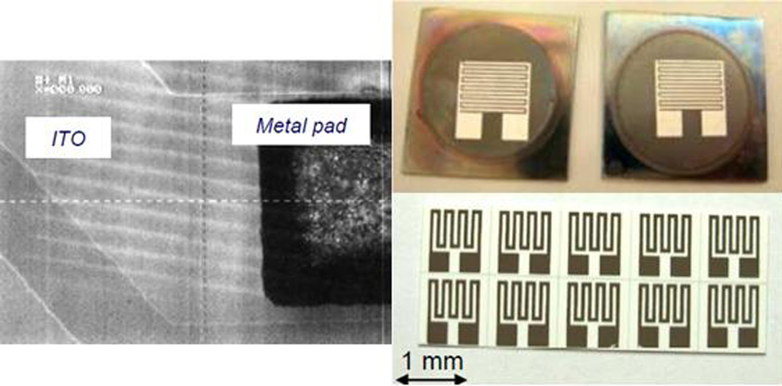
Figure 8. Tungsten nano pillars fabricated by material deposition using FIB Screen printing is another way to deposit a structured thin layer of a metal. CRF offers a screen printing machine, which allows deposition of different metals on several substrates (glass, alumina, silicon, metals and plastics). Figure 9 shows some examples of metals deposited using this technique.
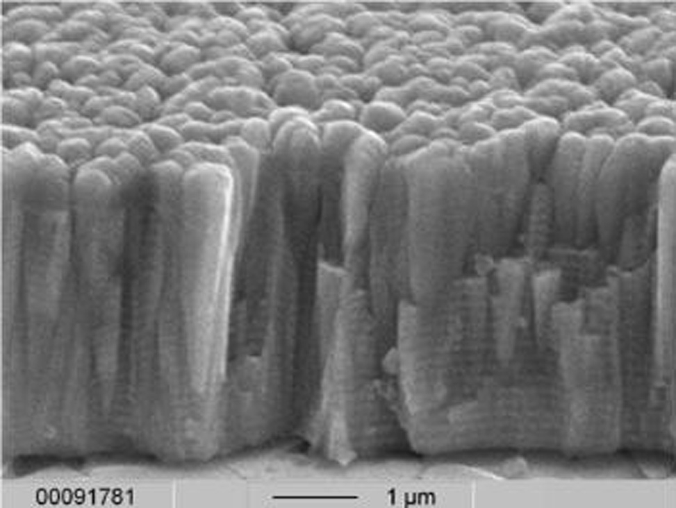
Figure 9. (Top) Aligned 20 µm silver pad on ITO track, (bottom) screen printed nickel on alumina and silver on porous titania for gas sensors In sensor technologies, ceramics are very useful crystalline materials because of their structural strength, thermal stability, light weight, resistance to many chemicals, ability to bond with other materials, and excellent electrical properties. Examples of ceramic materials are oxides, carbides and nitrides. For instance, alumina can be used as a humidity sensing compound, since its dielectric constant and surface resistivity are modified by the physisorption of water. Indium-tin oxide (ITO) can be used as a gas sensor, because its conductivity increases remarkably when exposed to reducing gases. Aluminum nitride and lead–zirconite–titanium oxides (PZT) are widely used for piezoelectric sensors. Thin films of ceramic materials can be deposited using reactive vapour deposition techniques, available in different locations at EUMINAfab. An example of a nitride film is shown in Figure 10.
Figure 10. Fracture surface of a TiN/ZrN multilayer coating Due to their hardness, most ceramics require special machining. A precise and cost-effective method of structuring and cutting ceramic substrates is laser micromachining. Micro-, pico- and femtosecond laser processing is offered at the installations of Cardiff University, KIT and Tekniker. Glasses can be also used in sensors, mainly as a substrate or as a protective layer. For example, metal oxide thermristors can be glass coated in order to provide them a long-term stability. Glasses can be machined in different ways and they can be deposited, growth or bonded. Anodic bonding is a popular method to bond silicon to glass. In this method a silicon wafer and a glass substrate are brought together, heated to a high temperature (400ºC) and an electric field is applied, causing a strong and irreversible bond between the two materials. It can be also remarked that besides other alternative approaches, EUMINAfab also offers dip-pen nanolithography. In this technique, the tip of an atomic force microscope is used to deliver molecular inks to a surface. It can deliver, for instance, thiols on gold or phospholipids with fluorescent or biotinylated groups on different substrates, so that it can be applied for biosensing. Finally, it must be added that, as in the case of the optical components, a large number of characterisation techniques are available to check the quality of the fabricated sensor components. Summary EUMINAfab provides open access to state of-the-art micro and nanotechnologies for a broad user community from industry and academia. A large number of the offered installations could be of great interest for optical and sensors fabrications. A detailed description of the equipment available for micro- or nanopatterning, thin film deposition, replication and characterisation, as well as the access conditions can be found on http://www.euminafab.eu. Acknowledgements EUMINAfab and its partners gratefully acknowledge the co-funding from the EC (Grant agreement no.: FP7-226460). Further to this stimulating funding several of the above mentioned developments are derived from other national or European projects, the contribution and collaboration of which are highly appreciated. References
|
| Legal notice |
|
| Related papers |
Presentation: Invited oral at EUMINAfab European research infrastructure for multimaterial micro and nano manufacture, by Jorge RamiroSee On-line Journal of EUMINAfab European research infrastructure for multimaterial micro and nano manufacture Submitted: 2010-07-07 18:17 Revised: 2010-08-19 12:28 |