Search for content and authors
 

In situ interferometry characterization of MOCVD grown ZnO on (100)-silicon

Jens-Peter Biethan ,  Laurence Considine ,  Dimitris Pavlidis 

Darmstadt University of Technology, Department of High Frequency Electronics, Merckstr. 25, Darmstadt 64283, Germany

Abstract

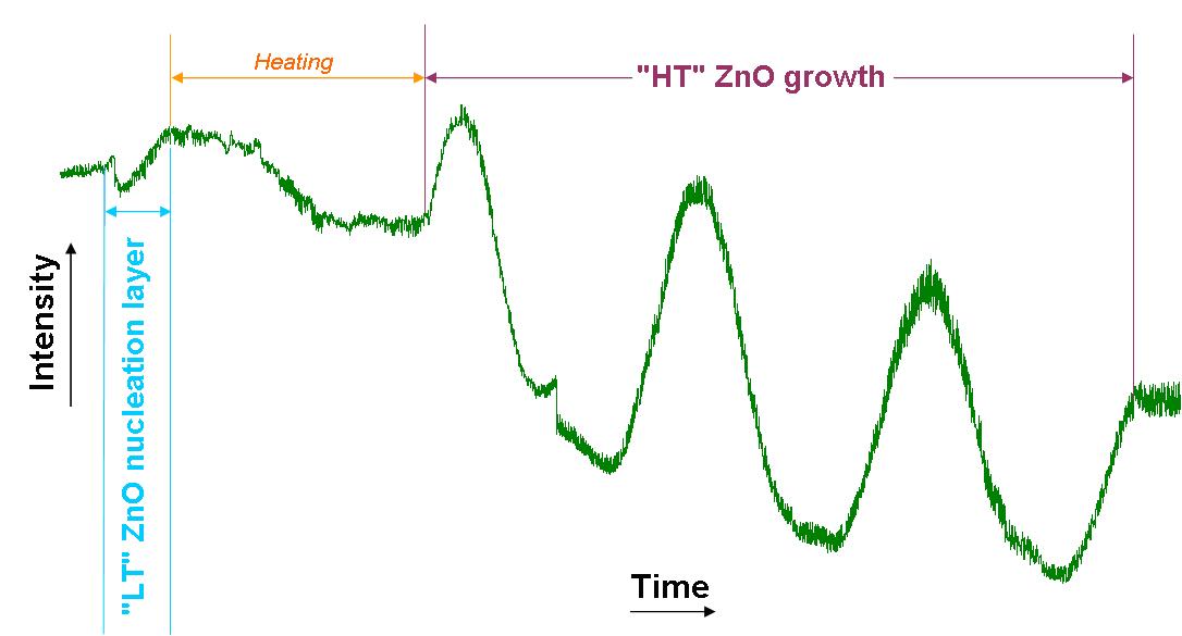
ZnO is an attractive transparent semiconductor material for electronic and optoelectronic applications. Compared to GaN, one of the major competitors of ZnO, ZnO has a higher binding energy, higher saturation velocity and exhibits better radiation hardness. ZnO has been already deposited on various substrates such as sapphire, glass or GaN, but only few reports exist on its deposition on silicon. The use of silicon as a substrate presents major advantages compared with other substrates. First, high quality silicon wafers can easily be obtained at low cost and second their resistivity can be relatively low.
Here we report the successful growth of ZnO on (100)-silicon wafers using an Aixtron 200 MOCVD system. To achieve good crystal quality and to address the issue of difference in crystal structure between the layers and the substrate, a low temperature nucleation buffer layer was first deposited on the silicon surface. Oxygen and DEZ were used as precursors while the carrier gas was selected to be nitrogen. The layer features were monitored using a homemade in situ laser interferometer. A red and a green laser were used for this purpose. To drastically minimise parasitic noise a notch filter was placed in front of a photodetector. A typical nucleation layer involves a two stage growth process where island formation results in reduction of reflectivity, followed by growth of either flat top areas covering the islands or of a planar layer leading to the start of an oscillation. A slight reduction of the reflected light intensity was observed shortly after DEZ was introduced. This effect could be described by diffusion scattering in the established Vollmer-Weber growth of islands. The subsequent increasing intensity of the laser signal marks the point were ZnO planar growth starts. High temperature ZnO layer growth starts following a heating step. Here typical well known thickness oscillations are observed by interferometry.

Fig. 1: Interferometer data LT and HT growth


Legal notice
  • Legal notice:
 

Related papers

Presentation: Oral at E-MRS Fall Meeting 2008, Symposium B, by Jens-Peter Biethan
See On-line Journal of E-MRS Fall Meeting 2008

Submitted: 2008-05-12 21:04
Revised:   2009-06-07 00:48