| Search for content and authors |
A High Temperature General Purpose Operational Amplifier with 300µA bias current and 4.5V to 20V Supply Voltage in Partially Depleted CMOS SOI |
| Gonzalo Picún , Aimad Saib , Laurent F. Vancaillie , Guillaume Pollissard , Nicolas Péquignot , Pierre Delatte , Vincent Dessard , Luc Maréchal , Laurent Demeûs |
|
CISSOID, Chemin du Cyclotron 6, Louvain-la-Neuve 1348, Belgium |
| Abstract |
1. Introduction Our new Operational Amplifier broadens the product offering of analog circuits specified for High Temperature operation, from -55°C up to 225°C. A high gain, low bias current, Gain-bandwidth product superior to 1MHz, reasonable offset and high output voltage dynamic range are results of the best technological trade-offs. 2. Circuit architecture and design The amplifier is based on a folded cascode architecture with Miller compensated class AB output stage, allowing a sufficient phase margin to be maintained independently of the output load. The design is made to keep a constant Gain-Bandwidth (GBW) product over temperature. No offset compensation scheme is used; a reasonable offset is guaranteed thanks to extensive Monte Carlo simulations and careful layout. 3. Current Consumption & Supply Voltage Single amplifier typical current consumption at 5V is 300µA at room temperature and rises up to 500µA at 225°C (see Figure 1). This current increase is necessary to guarantee a low drift of GBW product with temperature. 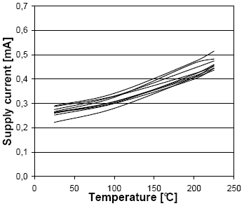
Amplifier operation is compatible with supply voltages from 4.5V up to 20V. The bias current slightly increases with the supply voltage as shown in Figure 2. 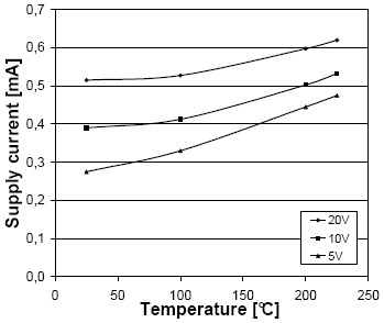
4. Gain High gain is achieved thanks to the folded cascode first stage. The gain at ambient temperature has been measured to be between 92 and 105dB for 10 samples and a high gain is maintained over the temperature range from 25°C to 225°C (Figure 3). 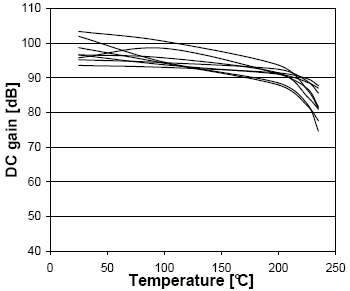
DC Gain behavior with supply voltage is rather constant. A gain drop of only 5dB can actually be noticed between low voltage operation and higher voltage operation. 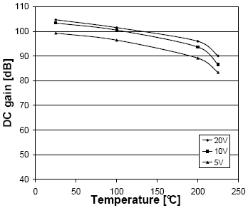
5. Gain-Bandwidth Product The Gain-Bandwidth (GBW) product was measured on ten samples loaded with a 2kOhms resistor and a 30pF capacitor, the amplifier being supplied at 10V. At 25°C (see Figure 5), the typical value is around 1.5MHz and rises to 1.7MHz at 225°C. 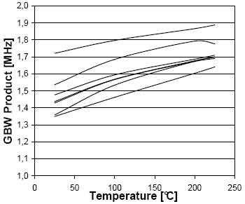
The impact of the supply voltage was also quantified (Figure 6): at low voltage (5V), the GBW product is 300 to 400kHz lower than at recommended voltage (10V). This evolution is due to the increase of the bias current. 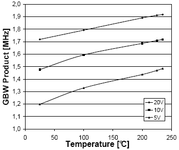
The GBW product was measured in the same conditions as in [1]: Rload=10kOhms, Cload=20pF and Vdd=10V. In this case, its value is equal to 1.65MHz and slightly increases with temperature. Figure 7 also shows how the Miller architecture allows maintaining a stable GBW product with the capacitive load. 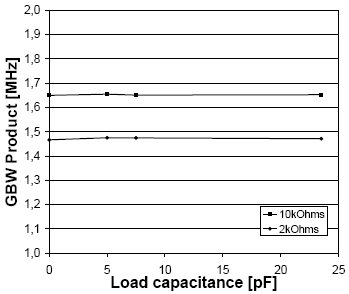
6. Offset Voltage Because CMOS transistors have relatively poor matching performance with respect to bipolar transistors, this amplifier only offers a moderate offset voltage performance. We kept out of any offset compensation scheme in order to not impact the circuit reliability and power consumption. A reasonable offset voltage is guaranteed thanks to extensive Monte Carlo simulations and careful layout. The histogram of the input offset voltage for 40 samples is shown in Figure 8. About 25% of the circuits have an offset voltage below 1mV and more than 90% below 4mV. 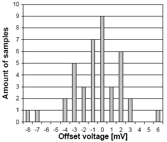
It is worth to mention for high temperature applications that the offset voltage decreases with temperature as shown in Figure 9. On this figure, we see that the worst case offset drift with temperature is 10.5µV/°C. 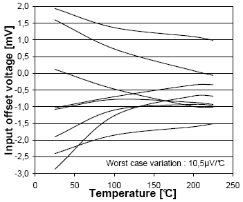
7. Slew Rate The slew rate versus temperature is shown in Figure 10 for a supply voltage of 10V, Rload=2kOhms in parallel with Cload=30pF. 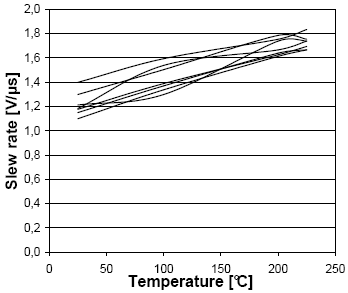
8. Packaging options The standard package is a DIL14 for a quad configuration. The circuit was also designed to be packaged in a DIL8 in a bi configuration. Other packages (SOIC, Metal CAN) are available on request. 9. Conclusions A new high temperature operational amplifier has been developed for general purpose use. The preliminary specifications are summarized in Table 1. It shows a good bandwidth and gain performance with low power consumption. A screening of components during test may produce parts with offset voltage in the 1mV range. Another advantage of the circuit is its ability to work properly at a low supply voltage of 5V. 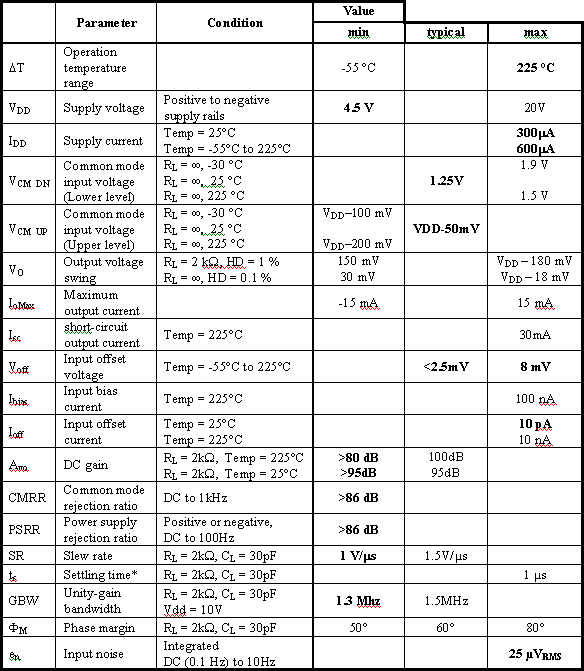
* Defined so that Vout reaches Vstep within 0.1 %, with Vstep = 1V in follower configuration. The values given are valid over the full temperature range (-55 °C to 225 °C) unless otherwise specified.
[1] HT1104 - HIGH TEMPERATURE QUAD OPERATIONAL AMPLIFIER Datasheet |
| Legal notice |
|
Presentation: Invited oral at HITEN 2007, by Pierre DelatteSee On-line Journal of HITEN 2007 Submitted: 2007-07-13 17:09 Revised: 2009-06-07 00:44 |