| Search for content and authors |
A SOI CMOS smart high-temperature sensor |
| Bertrand Rue , Denis Flandre |
|
Universite catholique de Louvain, Microelectronics laboratory (UCL), Place du Levant, 3, Louvain-la-Neuve 1348, Belgium |
| Abstract | ||
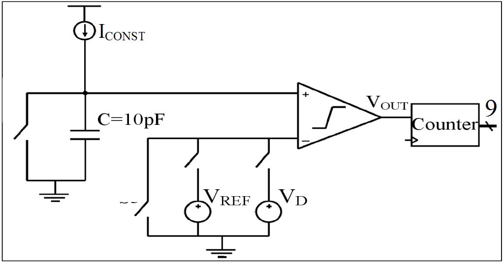
This paper reports the first SOI smart temperature sensor operating up to 250°C by integrating on the same chip the solid-state sensor itself (a SOI lateral PIN diode) and a simple digital conversion circuit. The sensor is implemented in a Fully-Depleted Silicon-On-Insulator process featuring a film thickness of 80nm [1]. Using the extraction method presented in [2], our non-gated PIN diode presents a quasi-linear temperature voltage characteristic when biased at a constant current (figure 1). The digital conversion circuit is shown in figure 2. The sensor output (figure 3) is the ratio of the time periods counted for the voltage on a reference capacitor charged by a constant current to reach respectively VD (diode voltage) and VREF (a Ultra-Low-Power reference voltage stable with temperature [3]) : α = TD / TREF The total power consumption of the circuit is 50µA*3V=150µW only. Despite the non-linearity of VREF , which is quite stable up to 200°C, the accuracy is 3°C in the range 25°C-250°C with 2 calibrations points (25°C, 200°C). For a fully-calibrated sensor, the maximum accuracy is 2°C with a resolution of 0.8°C. [1] D. Flandre et al.,“Fully-depleted SOI CMOS technology for heterogeneous micropower, high-temperature or RF microsystems”, Solid-State Electronics, -vol. 45, pp. 541–549, February 2001. [2] S. Adriaensen, D. Flandre, “High-Temperature Accurate Characterisation of SOI Bipolar/Diode Devices for their applications in Precise High-Order Bandgap References”, HITEN’03, Oxford, UK. [3] S. Adriaensen, V. Dessard, D. Flandre, “25 to 300°C ultra-low-power voltage reference compatible with standard SOI CMOS process”, Electronics Letters, vol. 38, issue 19, pp. 1103-1104, September 2002. 
Figure 1. Analog to Digital Converter.
| ||
| Legal notice |
|
| Related papers |
Presentation: Oral at HITEN 2007, by Bertrand RueSee On-line Journal of HITEN 2007 Submitted: 2007-07-13 15:59 Revised: 2009-06-07 00:44 |